The development of scalable quantum technologies depends not only on quantum processors, but also on the ability to read and control quantum states using practical semiconductor manufacturing processes.
A recent research commentary in Nature Electronics highlights an unexpected opportunity involving titanium nitride films already present in commercial CMOS fabrication processes.
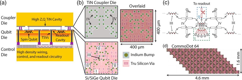
At millikelvin temperatures, these titanium nitride films can behave as high-impedance superconductors. This property enables them to function as compact inductive elements within semiconductor spin-qubit readout circuits.
The approach uses existing gate metallisation rather than requiring an entirely separate material system for the sensing component.
This is particularly interesting because semiconductor spin qubits are promising candidates for scalable quantum computing, but their measurement systems can require complex circuit architectures.
Integrating sensitive readout elements into existing chip structures could potentially reduce circuit complexity and improve the compatibility of quantum devices with established semiconductor fabrication technologies.
Engineering implications
The development connects semiconductor process engineering, superconducting materials and quantum-device architecture.
Using materials already available within a commercial CMOS process could provide a more practical route towards integrated quantum sensing.
However, the reported approach operates at extremely low temperatures, and significant engineering challenges remain in cryogenic operation, device integration, fabrication consistency and scaling.
It should therefore be viewed as a promising research direction rather than a commercially ready quantum sensor.
The broader lesson is that advanced electronic functionality may sometimes emerge from discovering new uses for materials already present in established manufacturing processes.